Sponsored by Renesas Electronics Corporation
In 2021, Renesas Electronics, one of the world's largest semiconductor companies with dominant automotive and industrial positions, significantly strengthened its IoT capabilities by acquiring Dialog Semiconductor. Dialog had built deep expertise in ultra-low power wireless connectivity and power management through strategic acquisitions and the successful SmartBond™ Bluetooth Low Energy product line, including the DA1453x SoC family, which consistently redefined industry benchmarks for power consumption and size.
This combination of Renesas' scale and manufacturing prowess with Dialog's wireless innovation creates comprehensive solutions spanning MCUs, wireless connectivity, and power management—positioning the merged entity as a formidable competitor in the rapidly expanding IoT market while maintaining Dialog's innovative edge in ultra-low power design.
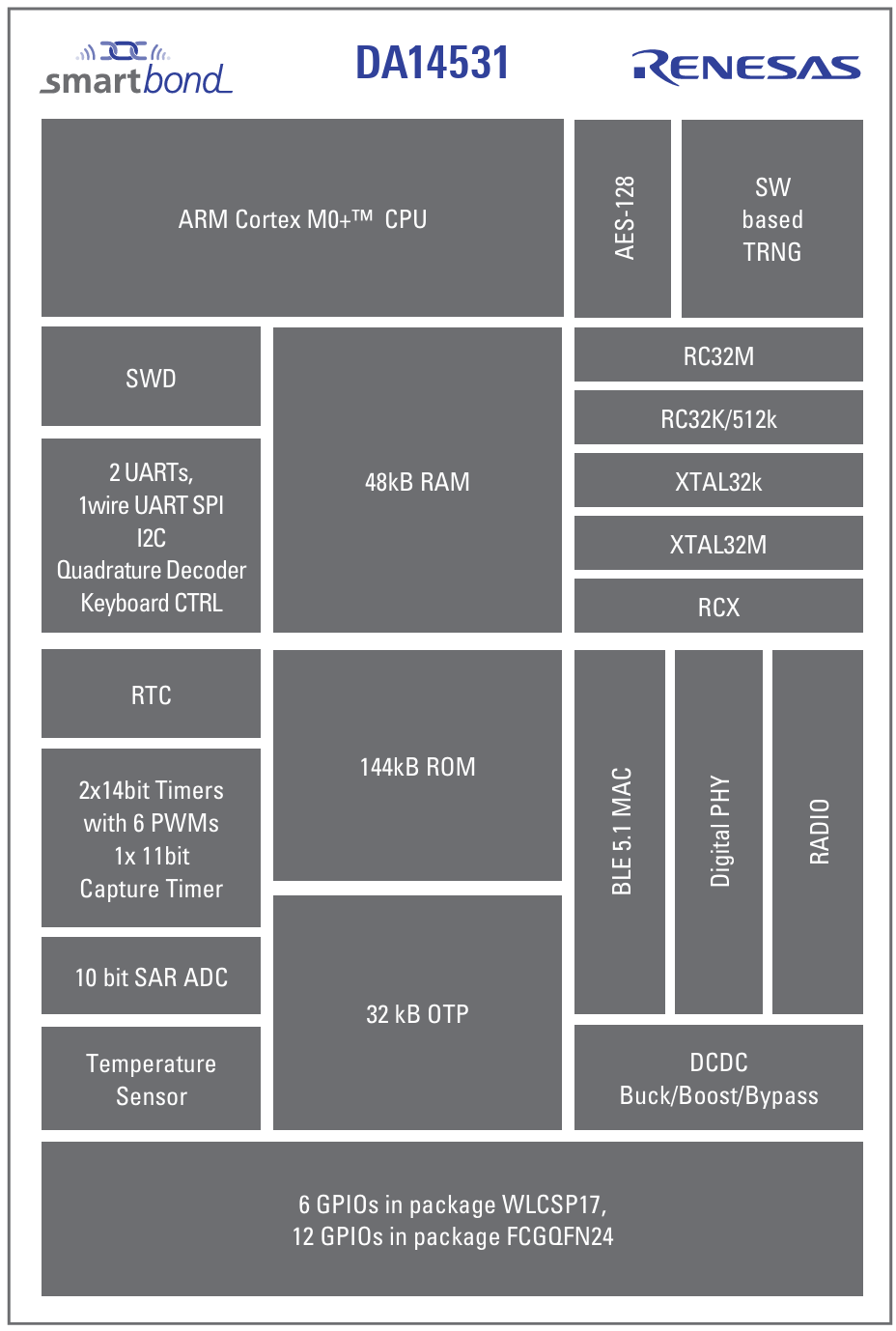
The Renesas DA1453x Bluetooth LE SoC family, led by the DA14531 "SmartBond TINY™", targets high-volume, cost-sensitive IoT applications through exceptional power efficiency and minimal system BOM. Built on Arm® Cortex-M0+ with dedicated hardware for BLE Link Layer and cryptographic functions, the DA14531 keeps the main CPU in deep sleep while its integrated PMU supports Buck, Boost, and Bypass modes for flexible battery options.
Rather than competing on raw performance, it dominates where power, size, and cost matter most—highly constrained designs previously out of reach. The development ecosystem combines SDK6, Keil µVision IDE, IAR, e² studio, and SmartSnippets™ tools with an event-driven architecture that maximizes the hardware's low-power capabilities.
Key Value Propositions
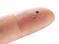
Ultra-Low Power in Minimal Form Factor: The DA14531 measures just 1.7mm × 2.05mm (WLCSP) while achieving 240 nA hibernation current, enabling operation from tiny batteries, including silver oxide and zinc-air. This unlocks disposable and space-constrained IoT applications previously deemed unfeasible.
Development-to-Production Flexibility: Start development with external Flash for over-the-air updates, then transition to cost-optimized OTP memory for production. This dual pathway supports both rapid prototyping and high-volume manufacturing economics, particularly valuable for disposable devices.
Renesas Ecosystem Integration: Functions as a standalone solution or Bluetooth LE coprocessor with Renesas MCUs through dedicated RA, RL78, and RX frameworks. Pre-certified modules eliminate RF design complexity while preserving existing MCU investments and providing clear upgrade paths.
Want to see the DA14531's ultra-low power performance and development workflow in practice?
Jump to our hands-on video demonstration →
Core Design Philosophies
To achieve its market-enabling goals, Renesas built the DA1453x architecture upon three uncompromising design philosophies: extreme power efficiency, minimal system cost, and simplified integration.
1. Extreme Power Efficiency
The paramount design constraint for the Renesas DA1453x family is power consumption. The SoCs explicitly target disposable products and operate effectively from the tiniest, disposable batteries, including silver oxide, zinc-air, and even experimental printed batteries with high internal resistance.
This focus is evident in industry-leading power efficiency, which ensures a long operating and shelf life, even with battery capacities below 30 mAh. The architecture's ability to limit inrush current is another critical feature that facilitates operation from these low-capacity power sources.
2. Minimal System Cost
The second pillar of the value proposition is an exceptionally low total system cost. A high degree of integration within the SoC itself achieves this. Developers can construct a complete and functional Bluetooth Low Energy system with the DA14531 and as few as six external passive components, a single 32 MHz crystal, and a power source.
This minimalist approach drastically reduces the Bill of Materials (BOM) cost, a critical factor for the high-volume, low-margin products it targets. Furthermore, certain variants and configurations, such as the DA14530 or using the DA14531 in bypass mode, eliminate the need for an external DC/DC inductor, further trimming the BOM for applications where power efficiency is a secondary concern to absolute cost.
3. Ease of Use and Integration
Recognizing that many potential adopters in high-volume markets may lack deep RF engineering expertise, Renesas has made ease of integration a central part of the platform's strategy. The most prominent example of this is the DA14531MOD, a fully integrated and pre-certified module.
This module incorporates the DA14531 SoC, all necessary passives, a crystal, external Flash memory, and an on-board antenna into a single, hand-solderable component. For product developers, this transforms the complex task of RF design, tuning, and regulatory certification into a "simple drop-in" solution, significantly reducing development costs, risk, and time-to-market.
This approach effectively lowers the barrier to entry, making sophisticated Bluetooth LE technology accessible to a much broader range of manufacturers.
4. System Integration Flexibility
The fourth cornerstone of the DA1453x architecture is its deployment versatility. The SoC family is engineered to excel in two distinct system configurations: as a standalone Bluetooth LE solution where the DA1453x handles all processing and connectivity functions, or as a dedicated Bluetooth LE coprocessor paired with a host MCU from Renesas's extensive microcontroller portfolio.
This architectural flexibility allows developers to optimize their system design based on specific requirements. Standalone deployment maximizes simplicity and minimizes BOM count, while coprocessor configurations leverage the computational power and peripheral richness of Renesas MCUs while offloading Bluetooth LE complexity to the specialized DA1453x. This dual-capability approach reduces development risk by allowing designers to migrate between architectures as product requirements evolve, while strengthening the overall Renesas ecosystem value proposition.
Deployment Flexibility: Standalone or Coprocessor Configurations
The DA1453x family's architectural design enables two distinct deployment strategies, each optimized for different application requirements and development workflows.
Standalone Configuration: Maximum Simplicity
In standalone mode, the DA1453x operates as a complete Bluetooth LE system, executing application code directly from its internal memory architecture. This configuration requires minimal external components—as few as six passive components plus a crystal and power source—making it ideal for cost-sensitive, space-constrained applications where simplicity is a priority.
The standalone approach is particularly well-suited for sensor nodes, beacons, simple HID devices, and disposable medical products where the application logic is relatively straightforward and the benefits of ultra-low power consumption and minimal BOM cost are critical.
Coprocessor Configuration: Leveraging the Renesas Ecosystem
Alternatively, the DA1453x can function as a dedicated Bluetooth LE coprocessor, connected to a host Renesas MCU via UART using the proprietary GTL (Generic Transport Layer) interface. In this configuration, the host MCU manages application logic, sensor interfacing, and complex processing, while the DA1453x handles all Bluetooth LE operations, including advertising, connection management, and data transmission.
This approach unlocks the full potential of Renesas's comprehensive MCU portfolio—from the ultra-low-power RL78 family to the high-performance RA and RX series—while providing seamless integration through the FSP (Flexible Software Package) framework. The coprocessor model is ideal for applications requiring complex processing, extensive peripheral interfacing, or integration with existing Renesas-based designs.
Strategic Flexibility and Risk Mitigation
The ability to choose between these deployment models—or even migrate between them during product development—provides significant strategic advantages. Developers can begin with a coprocessor approach during prototyping to leverage familiar MCU development tools and extensive peripheral libraries, then potentially consolidate to a standalone configuration for cost optimization in production. Conversely, products initially designed around the standalone DA1453x can easily scale up to coprocessor configurations if requirements expand beyond the SoC's integrated capabilities.
Architectural Deep Dive: The DA14531 SoC
The DA14531's architecture represents a carefully balanced system optimized for dual deployment scenarios: ultra-efficient standalone operation and seamless coprocessor integration within the broader Renesas ecosystem. Rather than a general-purpose microcontroller with attached radio, it is a specialized system engineered from the ground up for Bluetooth LE applications, whether operating independently or in partnership with a host MCU.
This architectural specialization is evident throughout the design—from the processing core and memory subsystem to the power management unit—with each element optimized to excel in both standalone and coprocessor configurations while maintaining the platform's core strengths of minimal power consumption, small physical footprint, and exceptional cost efficiency.
Did you know?
The DA14531 measures just 1.7mm × 2.05mm—smaller than a grain of rice—making it perfect for wearables, smart sensors, and space-constrained IoT devices!
Core Processing Unit: The Arm® Cortex-M0+
At the heart of the DA14531 is a 16 MHz 32-bit Arm® Cortex-M0+ processor. This core was selected for its exceptional energy efficiency and high code density rather than for raw computational power. It features a simple two-stage pipeline and implements the Thumb instruction set, achieving a performance metric of 0.9 DMIPS/MHz, which is more than sufficient for managing the Bluetooth LE stack and the simple sensor applications it targets.
A key architectural choice that enables the use of such a modest CPU is the offloading of critical tasks to dedicated hardware. The efficiency of this holistic system design is quantified by its EEMBC IoTMark™-Bluetooth LE score of 18300, a standardized benchmark that validates its leadership in IoT connectivity performance per watt.
Memory Subsystem: OTP, RAM, and ROM
The memory architecture is carefully partitioned to strike a balance between cost, flexibility, and power consumption.
- 32 kB One-Time-Programmable (OTP) Memory: This non-volatile memory is used to store the final application code, custom Bluetooth LE profiles, system configuration parameters, and device-specific calibration data. As its name implies, it can only be programmed once, a crucial consideration for manufacturing and production workflows.
- 48 kB Retainable System RAM: This is the primary execution memory. During the boot process, the application code stored in OTP (or external Flash) is mirrored into this SRAM, from which the CPU executes it. It also serves as data RAM for application variables and protocol data structures. The "retainable" nature of this RAM is critical for low-power operation; its contents can be preserved during sleep modes, allowing the device to wake and resume operation almost instantly without needing to perform a full reboot.
Unlike traditional MCUs with internal Flash, the DA1453x flash-less architecture reduces system cost, minimizes power consumption, and enables faster wake-up, while optional external Flash can be used for larger or updatable applications. - 144 kB ROM: The SoC includes a significant amount of read-only memory that contains the immutable bootloader sequence and the core, qualified Bluetooth LE protocol stack. Placing the stack in ROM reduces the amount of OTP or external Flash memory required for the user's application, contributing to a lower overall system cost and smaller code footprint.
Peripherals and Interfaces
Despite its small size, the DA14531 integrates a comprehensive set of peripherals to support a wide range of applications.
- Digital Interfaces: The number of available General Purpose I/O (GPIO) pins depends on the package: the ultra-small WLCSP17 package provides 6 GPIOs, while the larger FCGQFN24 package offers 12. Standard serial communication is supported by two UARTs (one with hardware flow control), an SPI Master/Slave interface capable of operating at up to 32 MHz in master mode, and an I2C bus supporting speeds of 100 kHz and 400 kHz.
- Analog Interfaces: The primary analog peripheral is a 4-channel 10-bit Analog-to-Digital Converter (ADC). It can be used to measure external analog sensors or internal signals, such as the battery voltage and the die temperature, providing essential system health monitoring capabilities.
- Timers and PWM: The SoC features two general-purpose timers with capture and Pulse Width Modulation (PWM) capabilities, making them suitable for tasks such as driving LEDs or controlling small motors.
Power Management Unit (PMU) and Consumption
The integrated Power Management Unit is arguably the most critical component of the DA14531's architecture, directly enabling its ultra-low-power performance and operational flexibility. The PMU manages all internal power domains and supports three distinct operating configurations based on the input power source.
- Buck Mode: Suitable for input voltages ranging from 1.8V to 3.6V, this mode utilizes a high-efficiency step-down DC/DC converter. This is the typical configuration for systems powered by lithium coin-cell or polymer batteries.
- Boost Mode: For very low input voltages, from 1.1V to 1.65V, this mode uses a step-up DC/DC converter. This capability is essential for enabling operation from single-cell alkaline or silver-oxide batteries.
- Bypass Mode: In this configuration, the DC/DC converter is disabled, and the system operates from an internal LDO. While less power-efficient, this mode offers the lowest BOM cost as it does not require an external inductor. This is a viable option for applications where cost is the absolute priority and battery life is less critical.
The PMU also orchestrates several power modes, allowing the system to shed power aggressively when idle. The current consumption figures demonstrate the SoC's extreme efficiency:
- Active Mode (Tx/Rx): 3.5 mA (transmitting at 0 dBm) and 2.2 mA (receiving).
- Extended Sleep Mode: With all 48 kB of RAM retained, the system consumes approximately 1.6 µA, allowing for very fast wake-up times.
- Hibernation Mode: In this clock-less state with no RAM retained, the SoC consumes a mere 240 nA to 270 nA, enabling multi-year shelf life on even the smallest batteries.
Radio Frequency (RF) Performance
The DA14531 features a fully integrated 2.4 GHz CMOS transceiver that is fully compliant with the Bluetooth 5.1 core specification. The design simplifies external circuitry by requiring only a single-wire antenna interface. Key RF performance metrics are highly competitive for their class:
- Receiver Sensitivity: -94 dBm, which allows for reliable communication over longer distances or in noisy environments.
- Transmit Output Power: Programmable from a very low -19.5 dBm up to +2.5 dBm, giving developers the flexibility to trade range for power consumption based on the application's needs.
Renesas DA1453x Family Variants
The DA1453x is not a single device, but a family of SoCs and modules, each tailored with specific feature sets and cost structures to address different market segments. Understanding the nuanced differences between these variants is critical for selecting the optimal component for a given application.
1. DA14531-00: The Baseline
- Full-featured device supporting both Central and Peripheral roles
- Complete feature set as described in the architectural overview
- Versatile choice for applications requiring connection initiation or discovery
2. DA14531-01: The Peripheral-Optimized Variant
- Peripheral-only operation (no Central or Observer roles)
- 25% more usable RAM compared to baseline
- Ideal for beacons, sensors, and tags that don't initiate connections
3. DA14530: The Cost-Optimized Variant
- Pin-compatible drop-in replacement for DA14531 in FCGQFN24 package
- Internal LDO instead of Buck/Boost DC/DC converter
- Eliminates the external inductor requirement for the lowest BOM cost
- Trade-off: reduced power efficiency versus DA14531
4. DA14535: The Bluetooth LE 5.3 Upgrade
- Bluetooth 5.3 compliance with future-proofing
- Increased system RAM (64 kB vs 48 kB) and higher transmit power (+4 dBm)
- Extended temperature range to 105°C for industrial applications
- Trade-offs: reduced OTP (12 kB vs 32 kB), no Link Layer Privacy
5. DA14533: The Automotive & Industrial Variant
- Same enhanced specifications as DA14535
- AEC-Q100 Grade 2 compliance for automotive applications
- 105°C operating temperature for harsh environments
DA1453x Family Comparative Specification Matrix
| Feature | DA14531-00 | DA14531-01 | DA14530 | DA14535 | DA14533 |
| Bluetooth Core Spec | 5.1 | 5.1 | 5.1 | 5.3 | 5.3 |
| Bluetooth LE Central Support | Yes | No | Yes | Yes | Yes |
| Bluetooth LE Observer Support | Yes | No | Yes | Yes | Yes |
| LL Privacy | Yes | No | Yes | No | No |
| System RAM | 48 kB | 48 kB | 48 kB | 64 kB | 64 kB |
| OTP Memory | 32 kB | 32 kB | 32 kB | 12 kB | 12 kB |
| ROM | 144 kB | 144 kB | 144 kB | 160 kB | 160 kB |
| PMU | Buck/Boost DCDC | Buck/Boost DCDC | LDO (Bypass) | Buck/Boost DCDC | Buck/Boost DCDC |
| Max Output Power | +2.5 dBm | +2.5 dBm | +2.5 dBm | +4 dBm | +4 dBm |
| Temp Range (°C) | -40 to +85 | -40 to +85 | -40 to +85 | -40 to +105 | -40 to +105 |
| Package(s) | FCGQFN24, WLCSP17 | FCGQFN24, WLCSP17 | FCGQFN24 | FCGQFN24 | FCGQFN24 |
| AEC-Q100 | No | No | No | No | Yes (Grade 2) |
| Module Available | DA14531MOD | —— | —— | DA14535MOD | —— |
Choosing Your DA1453x Variant:
For the simplest implementation and lowest BOM cost: Choose DA14530 when external inductor elimination is a priority and moderate power efficiency is acceptable.
For ultra-low power sensors, beacons, and tags: Choose DA14531-01 when devices only need to advertise or be connected to (not initiate connections), and maximum RAM is beneficial.
For versatile standalone applications: Choose DA14531-00 when you need full Central/Peripheral capability and a proven, mature platform with maximum flexibility.
For future-proofed or industrial applications: Choose DA14535 when Bluetooth 5.3 compliance, higher transmit power, or extended temperature operation is required, and a smaller OTP is acceptable.
For automotive applications: Choose DA14533 when AEC-Q100 compliance and harsh environment operation are mandatory requirements.
Architecture Decision:
- Standalone configuration: Simple sensors, beacons, HID devices, or disposable products with straightforward application logic
- Coprocessor configuration: Complex processing requirements, extensive peripheral interfacing, or integration with existing Renesas MCU-based designs
The Developer Experience: Ecosystem and Software Architecture
A successful SoC is defined not only by its hardware capabilities but also by the quality and accessibility of its software ecosystem. Renesas provides a comprehensive suite of tools and software for the Renesas DA1453x family, designed to support developers from initial prototyping through to mass production.
The Renesas SmartBond DK6
The foundation of software development for the Renesas DA1453x family is the SDK6, a comprehensive software development kit that includes the Bluetooth LE stack, peripheral drivers, and a rich set of example applications. A key architectural element of the SDK is its use of a small and efficient Real-Time Kernel (RTK).
This is not a full-featured real-time operating system (RTOS), but rather a lightweight scheduler. The entire Bluetooth LE stack and the user application are structured as a series of independent tasks that communicate via messages and events handled by the kernel. This event-driven, message-passing architecture is a direct software reflection of the hardware's low-power design philosophy.
The main application loop consists of the kernel's scheduler, which processes all pending events in its queues (such as incoming Bluetooth LE packets, timer expirations, or application messages). Once the queues are empty, there is no more work to be done, and the scheduler immediately allows the system to enter a low-power sleep mode. This tight coupling between the software paradigm and the hardware's capabilities is fundamental to achieving the ultra-low power performance that defines the platform.
Renesas SmartBond SDK6 Unique Features
The SDK6 also includes several high-level features to accelerate development.
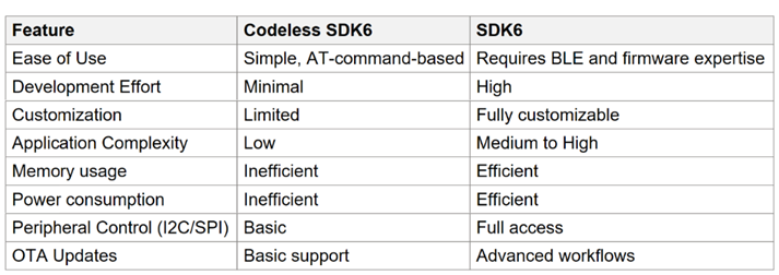
CodeLess AT Command Interface
The CodeLess AT command interface is a ready-to-use firmware solution for the DA1453x family, providing a simple way to control the SoC via AT commands over serial interfaces and/or BLE. It abstracts away low-level Bluetooth LE programming, allowing system designers and application developers to quickly configure and operate the device without writing embedded code. This makes it particularly useful for rapid prototyping or for “Bluetooth LE pipe” applications where the DA1453x is paired with a host MCU.
When NOT to use Codeless
- Advanced or Custom BLE Features
- High-Performance Applications with low latency; avoid AT command interpretation overhead
- Memory-constrained application
- Complex peripheral interfacing for efficient and real-time sensor data transmission
Serial Port Service (SPS)
SPS (Serial Port Service) is a Bluetooth LE-based UART-to-serial bridge developed by Renesas Electronics. It allows wireless transmission of serial data over Bluetooth Low Energy, functioning similarly to a Classic serial (UART) connection but over Bluetooth LE.
When to use SPS
- When you need UART-to-Bluetooth LE functionality
- For quick prototyping of serial data transfer
- When monitoring throughput or testing a Bluetooth LE link performance
- When replacing wired serial communication with Bluetooth LE
When NOT to use SPS
- While SPS is not only for monitoring throughput, it is mainly used for transparent serial data transmission rather than full-fledged Bluetooth LE application development.
- If your application requires custom BLE services or complex logic
- When optimizing low power (SPS may not be the most efficient)
- If you need bidirectional control signals beyond just serial data
Software Update Over-The-Air
- The SDK also provides robust support for Software Update Over-The-Air (SUOTA), which is a critical feature for deploying firmware updates to devices in the field. This requires an external flash, which is used for storing the application image that gets executed from there or copied into system RAM for execution. In this scenario, the OTP could still be used for other important system data, such as configuration and/or calibration data.
References:
- CodeLess AT command interface: https://www.renesas.com/en/software-tool/smartbond-codeless-commands
- SPS: https://www.renesas.com/en/software-tool/serial-port-service-sps
- Software Update Over-The-Air (SUOTA): https://lpccs-docs.renesas.com/Tutorial_SDK6/suota_overview.html
The Development Tools Ecosystem
The development toolchain for the Renesas DA1453x provides comprehensive coverage through specialized tools, each serving distinct and complementary roles in the development workflow:
- e2 studio: This is Renesas’s royalty-free, Eclipse-based IDE, providing a complete development environment with a project manager, editor, and debugger. The DA14531 SDK6 includes full support for e² studio and the LLVM compiler, offering enhanced development capabilities. e² studio is suitable for both evaluation and professional, long-term development, with no code-size limitations.
- SmartSnippets™ Toolbox is a utility suite included with Renesas Bluetooth development kits, designed to simplify development and optimize applications for ultra-low-power performance. It provides full visibility into chip activity and leverages the motherboard’s features, eliminating the need for costly external equipment. Key tools include:
- Programmer: A graphical tool for programming firmware into the SoC’s internal SRAM, OTP, or external SPI/I2C Flash memory. It is the primary tool for production programming.
- Power Profiler: Interfaces with the development kit’s current measurement hardware to provide a real-time, high-resolution view of the SoC’s power consumption. Developers can see the impact of code changes instantly and optimize for maximum battery life.
- Keil® µVision: This is the most common Integrated Development Environment (IDE) for getting started with the Renesas DA1453x. The vast majority of Renesas's official tutorials and example projects are provided as Keil µVision projects. A free version of the Keil MDK-ARM toolchain is sufficient for building and debugging these examples, making it an accessible entry point for new developers.
Production Line Tool (PLT)
Renesas provides a production testing and programming solution that helps reduce costs and speed up production. The Connectivity Production Line Tool (PLT) is a flexible system that makes it easier to test and program devices built with Renesas DA1453x Connectivity ICs.
The PLT can test, calibrate, and perform memory operations on several devices at the same time. For example, you can connect to four PLT boards, each with eight test sites, allowing up to 32 devices to be tested at once. This setup helps increase efficiency in high-volume production.
Development Hardware
Renesas provides a couple of hardware platforms to facilitate development with the Renesas DA1453x family.
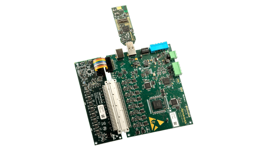
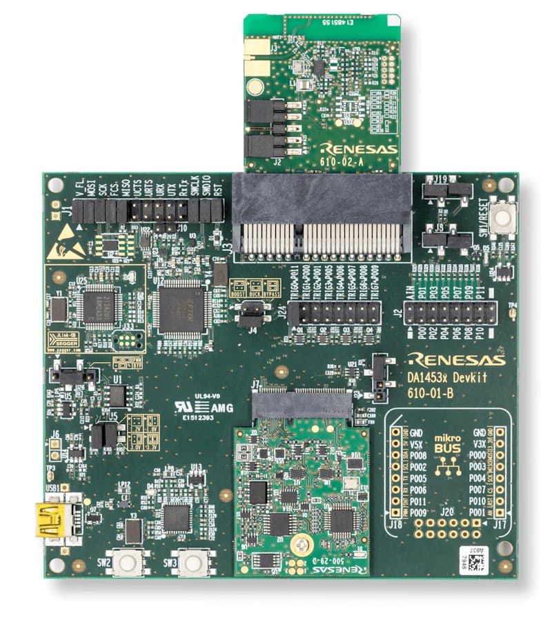
- DA14531 Development Kit Pro: This is the primary development platform, offering maximum flexibility and functionality. It consists of a large motherboard and a small, interchangeable daughterboard that holds the specific DA1453x SoC variant. The motherboard includes an onboard Segger J-Link debugger, a USB-to-UART bridge, user-configurable buttons and LEDs, and, most importantly, dedicated circuitry for precise current measurement that integrates with the SmartSnippets™ Toolbox Power Profiler.
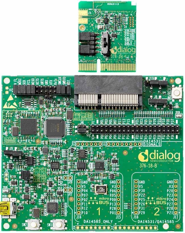
- DA14535 Development Kit Pro: The DA14535-00FXDEVKT-P Bluetooth® Low Energy Development Kit Pro for the DA14535 SmartBond TINY™ SoC includes a motherboard, daughterboard, and cables. This kit is primarily intended for software application development and power measurements.
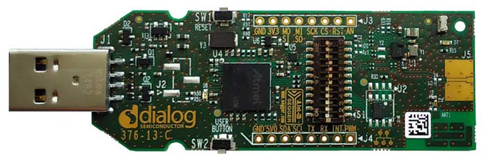
- DA14531 USB Development Kit: This is a much smaller, self-contained "dongle" style board. It integrates the DA14531 SoC and a USB connector onto a single PCB, making it a convenient and low-cost option for simpler prototyping and software development where advanced power measurement is not required.
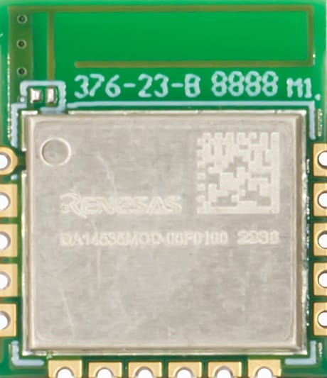
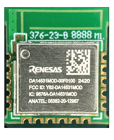
- DA14531 Module: The DA14531 SmartBond TINY™ Module leverages the world's smallest, lowest-power Bluetooth 5.1 SoC in an integrated package. With regional certifications, an integrated antenna, and user-friendly software, it significantly reduces development costs and time-to-market. The module requires only a power supply and PCB to create Bluetooth applications, making BLE development more accessible for broad market deployment.
- DA14535 Module: The DA14535MOD is a globally certified, ultra-low-power Bluetooth® Low Energy v5.3 module designed for cost-effective wireless connectivity. Perfect for rapid product upgrades, it enables smartphone integration for commissioning, control, alerts, and data collection. As a pin-compatible alternative to the DA14531MOD, it features a Cortex-M0+ processor operating at 16MHz, integrated 1Mbit Flash, RAM/ROM/OTP memory, a 32MHz crystal, a power inductor, RF matching, and a printed antenna—all in a fully self-contained package.
Mobile App Tools
In addition to the PC-based software tools available (IDE, SmartSnippets™Toolbox, etc.), Renesas offers a Bluetooth Low Energy explorer application, available on both iOS and Android:


DA1453x SoC as a Network Coprocessor
Renesas Ecosystem Integration
The DA1453x family's coprocessor capability represents a strategic integration point within the broader Renesas semiconductor ecosystem, enabling customers to leverage decades of microcontroller expertise while adding best-in-class Bluetooth LE connectivity.
Architecture and Communication
In coprocessor mode, the DA1453x firmware is stored in the host MCU's flash memory and loaded into the DA1453x RAM at boot time. The two processors communicate via a 4-wire UART interface using Renesas's proprietary GTL (Generic Transport Layer) protocol, which provides native support for all Bluetooth LE operations, including advertising, connection management, security procedures, and data transfer.
This architecture allows the host MCU to maintain complete control over Bluetooth LE functionality while offloading the complexity of RF management, protocol stack execution, and regulatory compliance to the specialized DA1453x hardware.
Renesas MCU Family Support
The coprocessor implementation is supported across Renesas's major MCU families through dedicated software frameworks:
- FSP (Flexible Software Package) Framework: Comprehensive support for RA Arm Cortex-M MCUs with integrated Bluetooth LE APIs and example applications
- RL78 Framework: Optimized integration for ultra-low-power RL78 applications where both processors can cooperate to minimize system power consumption
- RX Framework: High-performance integration for applications requiring significant computational capabilities alongside Bluetooth LE connectivity
Strategic Advantages
This coprocessor approach delivers several key benefits: it preserves existing investments in Renesas MCU expertise and codebases, enables rapid integration of Bluetooth LE into established product lines, provides access to the extensive peripheral capabilities of Renesas MCUs, and creates clear upgrade paths as product requirements evolve. The unified Renesas ecosystem also simplifies supply chain management, technical support, and long-term roadmap alignment.
For more information about this setup, refer to the following user guides:
- Getting Started with DA1453x and FSP Bluetooth Low Energy Framework on Renesas Microcontrollers
- Getting Started with DA1453x and RL78 Bluetooth Low Energy Framework on Renesas Microcontrollers
- Getting Started with DA1453x and RX Bluetooth Low Energy Framework on Renesas Microcontrollers
Real-World Products Utilizing the DA1453x SoC Family
The Renesas DA1453x family's specific focus on ultra-low power, minimal size, and low system cost has led to its adoption in a wide array of commercial products and reference designs. Here is a summary of products and companies that utilize this SoC family.
Consumer and Smart Home Products
The DA1453x family is frequently used in high-volume consumer electronics where long battery life and a small form factor are critical selling points.
- HyperSynes Smart BBQ Thermometers: HyperSynes, a global leader in smart grilling technology, uses the Renesas DA14531 in its advanced smart meat probes and BBQ temperature controllers. The SoC's ultra-low power consumption and compact design were crucial for creating completely wireless, slim, and highly accurate food thermometers. According to HyperSynes, their products, powered by the DA14531, are used in 95% of the world's wireless food thermometers, sold under their own name and through private-label brands.
- Human Interface Devices (HID): The SoC's efficiency makes it ideal for peripherals such as electronic styluses, wireless keyboards, computer mice, and remote controls that replace traditional infrared (IR) versions.
- General Consumer Goods: The DA1453x is also found in products like smart toys, smart credit cards, and as a simple "Bluetooth LE pipe" to add connectivity to existing applications with a host microcontroller.
Connected Medical and Health Devices
The DA1453x family is explicitly optimized for the connected medical market, particularly for disposable or single-use products where cost and the ability to operate from small, non-rechargeable batteries are paramount.
- Disposable Medical Devices: The SoC is designed to be integrated into products such as connected injectors, inhalers, glucose monitors, smart patches for vitals monitoring, blood pressure meters, and digital thermometers. Its ability to operate from specialized power sources, such as silver oxide, zinc-air, or even printed batteries, makes it uniquely suited for this category.
Asset Tracking, Beacons, and Logistics
The combination of low power for extended shelf life and small size for discreet placement makes the DA14531 a popular choice for tracking and proximity applications.
- Nodle N1 NanoComputer: Nodle uses the DA14531 "SmartBond TINY™" as the core of its N1 NanoComputer, a device designed for its decentralized IoT network. This network is used in applications such as locating and recovering stolen vehicles for insurance companies. Nodle selected the DA14531 for its low-power operation, encryption capabilities, cost-effectiveness, and robust performance, which were essential for creating a programmable, low-power edge computing device.
- Feasycom Bluetooth Beacons: Feasycom, a provider of IoT modules and solutions, partnered with Renesas to create a line of high-performance Bluetooth beacons based on the DA14531. Feasycom chose the DA14531 over competing solutions because its power consumption is roughly half that of alternatives, effectively doubling the battery standby time. This advantage, combined with the SoC's small size and high return on investment, was critical for their product strategy.
- Renesas Smart Asset Tracking Label: As part of its "Winning Combinations" portfolio, Renesas features a credit card-sized smart tracking label. This reference design uses the DA14531 SoC with Renesas humidity and temperature sensors to monitor environmental data. The design achieves a 2-3 month shelf life and around 30 days of active use from a small 25mAh printable battery.
- Hongjia Electronic Technology Modules: Hongjia’s journey with Renesas began in 2014 when the company adopted the DA14580 System-on-Chip (SoC) to develop the HJ-580 series of modules. Building on this success, Hongjia continued to innovate with the introduction of the HJ-131IMH and HJ-531IMF Bluetooth® Low Energy (LE) modules in 2020, based on Renesas’ DA14531.
- DX Smart Technology, a company specializing in wireless communication modules and solutions, joined forces with Renesas Electronics. By incorporating Renesas’ cutting-edge System-on-Chips (SoCs) into their products, DX Smart has not only streamlined its research and development but also provided unparalleled value to customers seeking competitive advantages through quick validation and reduced costs.
Automotive and Industrial Applications
While the family broadly targets consumer and medical markets, its reliability and efficiency also suit certain automotive and industrial use cases.
- Tire Pressure Monitoring Systems (TPMS): The DA1453x family is frequently listed as a suitable component for TPMS applications, where low power consumption is necessary to maximize the battery life of sensors mounted inside tires.
- Low-Power Wireless Sensors: The SoC is also used in various low-power wireless sensors for industrial monitoring applications.
How to Get Started with Development for the DA14531 SoC
Hardware Prerequisites
- Computational workstation (for example, PC or Laptop)
- 32-bit or 64-bit processor with 1 GHz processing speed
- 1 GB RAM
- 2 GB free disk space
- DA14531-00FXDEVKT-P as a motherboard
- DA14531-0x daughterboard FCGQNFN 24 package (DA14531-00/DA14531-01- QFN daughterboard).
- USB cable for power supply to the Pro Development kit and for on-board debugging
Software Prerequisites
To get started, download the following software packages:
- Software Development Kit (Renesas SmartBond SDK)
- e² studio (you can also use Keil)
- SmartSnippets™ Toolbox
- Keil MDK ARM (you can also use e² studio)
- FTDI Driver for Windows
- Segger J-Link SW driver
Video Tutorial/Demo
Summary
The Renesas DA1453x Bluetooth LE SoC family, led by the DA14531 "SmartBond TINY™", represents a breakthrough in ultra-low-power wireless connectivity for cost-sensitive IoT applications. Built on Arm® Cortex-M0+ architecture with dedicated BLE hardware, these SoCs achieve industry-leading hibernation currents as low as 240 nA while requiring just six external components for a complete system.
The family's three core design philosophies—extreme power efficiency, minimal system cost, and simplified integration—enable operation from tiny batteries (including silver oxide and zinc-air) and make Bluetooth LE accessible for previously unfeasible applications. With variants optimized for different use cases (peripheral-only, cost-optimized, automotive-grade), comprehensive SDK6 development tools, and pre-certified modules, the platform has achieved widespread adoption in smart home devices, medical wearables, asset tracking, and automotive applications.
This deep dive explored the architectural innovations, power management techniques, family variants, development ecosystem, and real-world implementations that position the DA1453x as the go-to solution for battery-powered IoT devices where every microamp and penny counts.
Resources and Links
DA1453x SoCs
- Product Selector: https://www.renesas.com/en/products/wireless-connectivity/bluetooth-low-energy/product-selector?product-id=da1453
- DA14531 product page: https://www.renesas.com/en/products/da14531
- DA14530 product page: https://www.renesas.com/en/products/da14530
- DA14533 product page: https://www.renesas.com/en/products/da14533
- DA14535 product page: https://www.renesas.com/en/products/da14535
- DA14531 Datasheet: https://www.renesas.com/en/document/dst/da14531-datasheet?r=1564826
SDK6
- DA1453x/DA1458x Tutorial SDK6 Getting Started: https://lpccs-docs.renesas.com/Tutorial_SDK6/index.html
- Download SDK6: https://www.renesas.com/en/document/swo/sdk60241464-da1453x-da145856
- SDK6 Examples: https://github.com/renesas/ble-sdk6-examples
Development
- e2 studio: https://lpccs-docs.renesas.com/e2_studio_sdk6_getting_started/index.html
- Renesas DA Tutorials: https://lpccs-docs.renesas.com/lpc_docs_index/DA145xx.html#tutorials
- DA14531 Getting Started with the Pro-Development Kits: https://lpccs-docs.renesas.com/UM-B-117-DA14531-Getting-Started-With-The-Pro-Development-Kit/index.html
Bluetooth Low Energy Technical Support Community
End-product Example
Renesas Partner Program